ONE-O-SIX KIT ASSEMBLY & CALIBRATION
We strongly advise you to fully read (several times !) the whole assembly process before starting any soldering. Notice you need a very few tools and understand a bit how the chorus works (power supply, effect on, the level meter, control of the modulator LFO).
The unit needs some calibrations to be fully operative. You will calibrate the LEVEL meter and the two BBD delay (a chorus is a variable short delay) circuits. For this you need a test signal -usually a sinus signal or at least a saw/triangle one- produced by a signal generator (your DAW has one, Yamaha mixers have one, etc). An oscilloscope or a software oscilloscope might be sufficient or you can use your ears if you are trained to analyse audio signal.
ABSOLUTELY NECESSARY TOOLS :
- solder iron,
- solder,
- tweezers,
- 8 pieces of M3x30mm (or longer) M/F stand off,
- +9VDC 1Amp, center negative, power supply (e.g BOSS PSA),
- adhesive tape.
DOCUMENTATION
Get your components according the Bill Of Material :
definitive BOM for PCB REV3 and REV3.1 Alpes_Machines-One_O_Six-Chorus 13dec2019
Fabrication files – parts value and reference on the printed circuit board :
Alpes_Machines-One_O_Six-Chorus-brd_TOP
Alpes_Machines-One_O_Six-Chorus-brd_BOTTOM
Schematic rev3.1 : take a look on it to understand how the jumpers and Test Points TP are used. We recommend you to print it (A3 size) :
Alpes_Machines-One_O_Six-Chorus
Enclosure files :
1590XX ONE-O-SIX_CAD 1590XX ONE-O-SIX
TEST POINT : AUDIO & VOLTAGES
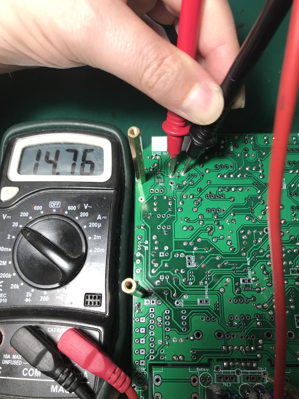
You can test the voltages on board :
- Ground : TP3, TP11,P6 (P6 can be used to connect the ground of your oscilloscope/voltmeter)
- +15VDC : TP4, TP9
- -15VDC : TP5, TP10
NOTA : voltages are created by the small DC_DC 3W board and are not exactly +/-15.00VDC. We have measured +14.76VDC and -14.61VDC while the assembly of the prototypes. The manufacturer specifies -5% for the negative voltage in comparison to the positive one.
P5, P7 are additional connectors to the +/-15.00VDC power supply lines. You can use them to power another circuit like a signal generator.
You can test the audio signal path :
- audio input : TP6 INPUT, P8 (Ground, Mono)
- chorused audio channel A : TP7 A OUT (Left)
- chorused audio channel B : TP8 B OUT (Right)
- audio outputs : P9 (Right, Left, ground)
You can test the LFO (with RATE & DEPTH potentiometers soldered) :
- normal LFO (for voice A) : TP1 LFO
- inverted LFO (for voice B) : TP2 i-LFO
ALTERNATIVE PARTS & MODS :
Parts with a value* (marked with an asterisk) are optional and/or can be changed to fit different Juno/JX chorus design :
- R80 = 33K if your synths don’t send high level signal or use 22K for less gain and thus use the whole gain knob range.
- R118 = 1K* or wire. See the different LFO designs regarding the corresponding synth.
- D20 = 1N4148 only used in Roland Juno 106 design. replace with a wire for other designs.
- R25 = 2M2* used in Juno 106 design. A higher value produces slower LFO rates (e.g 3M3) while a lower value produces faster LFO (e.g 1M in Boss CE-2).
- R114 = 1K* to avoid a zero DEPTH value. can be swapped for a wire.
- C60 et C56 = 100uF used to filter clock leakage when using MN3007. Omit them if MN3009 is used.
- C59 = 2n2 : ommited in the original Juno106 chorus voice A design despite existing on the Juno 106 chorus voice B (Roland error or filtering of inverted LFO in conjunction of C62 = 220pF* ?).
- C62 = 220pF* need to be set in correlation of value R43/R38 to remove transients when inverting i-LFO (complicated, this depends of TL0xx and resistors value, more on that later). Leaving it free is the easiest.
- R57 = 1K* used to protect input of transistor driving the LFO LED.
- C42 = 10nF* and R110 = 100K* are used in Boss CE300 to filter Schmidt trigger state transitions thumps (low cut filter). R110 is a wire in Roland Juno 106 design. Implement them like this helps a lot to reduce low frequency thump in the clock and thus the chorused signal.
- R_MUTE, R_LFO, R_ON, R_PWR are used to protect the corresponding LEDs. A 10K value is fine, use higher value to diminish LEDs shining.
- R103, R108, R106, C41 (R102, R107, R104, C40) are used to create Juno 106 output stage. This creates a 1/1 gain input/output level. Populate them or replace with wires R102/R107, R103/ R108 and let the rest free.
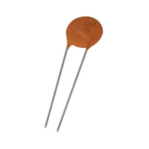
- BP : bypass capacitors they are small cheap ceramic disc capacitors like image below, used to decouple the power supply lines, with a value of 100 nF (104Z)
*****more to come later*****
Count and sort your components by category (resistors, capacitors, IC, etc) :
**picture of components bags**
The different steps to solder and assemble your unit :
- small passive components
- power supply section
- large passive components
- active components and Integrated circuits
- calibrating
- enclosure
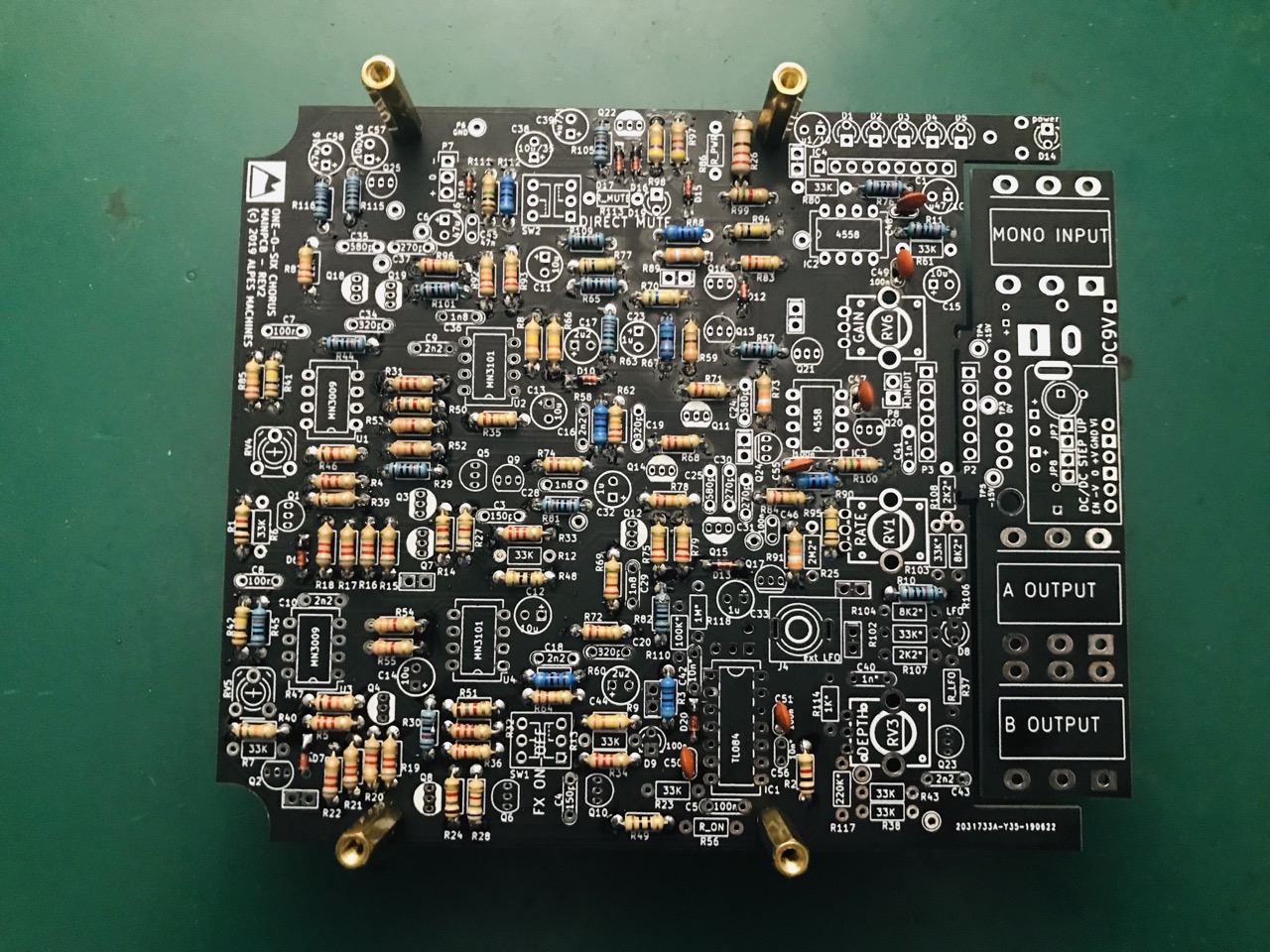
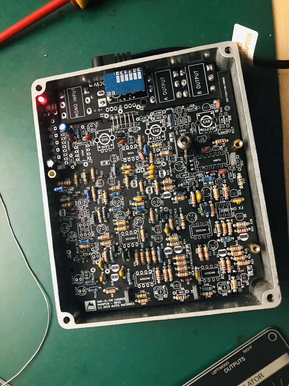
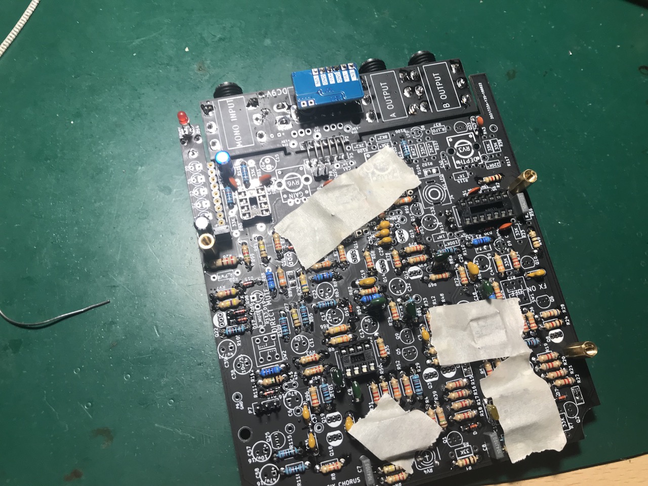
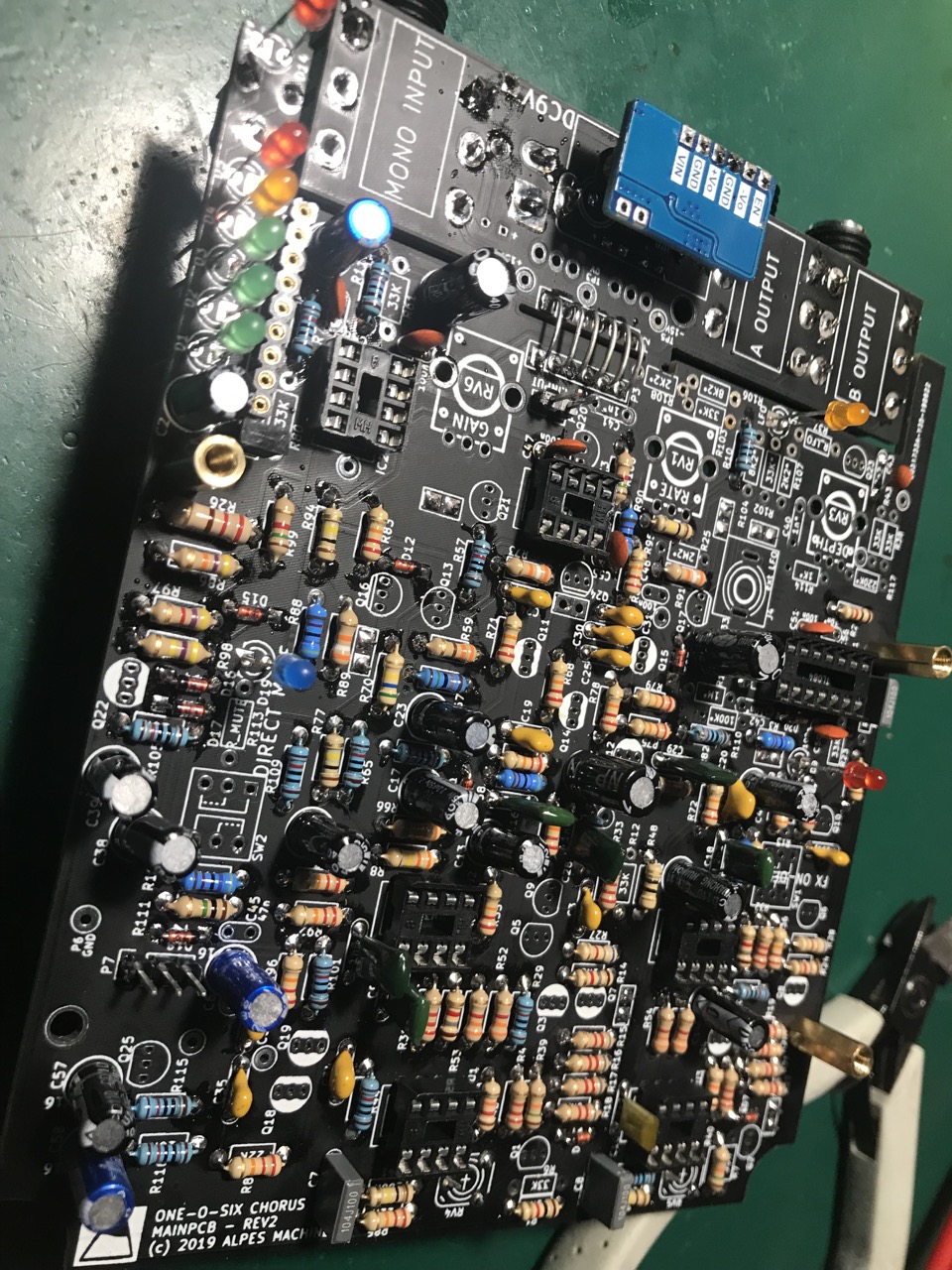
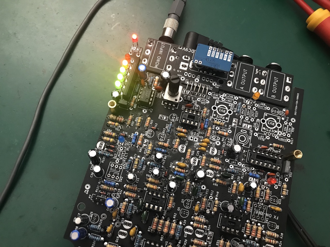
ASSEMBLY of the REV2 board (not commercialized) : black PCB. Presented here for your information and an introduction how to populate the board.


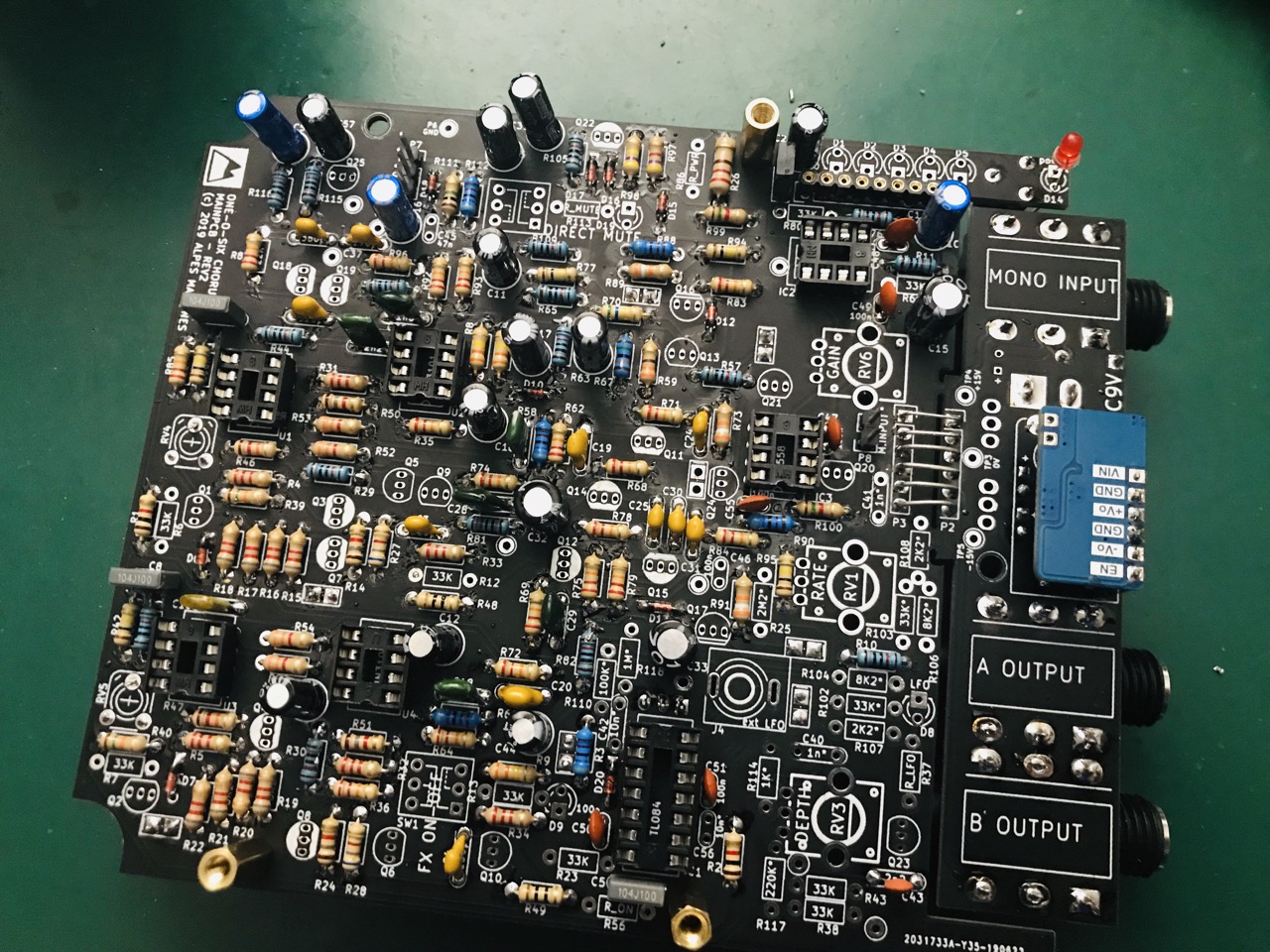

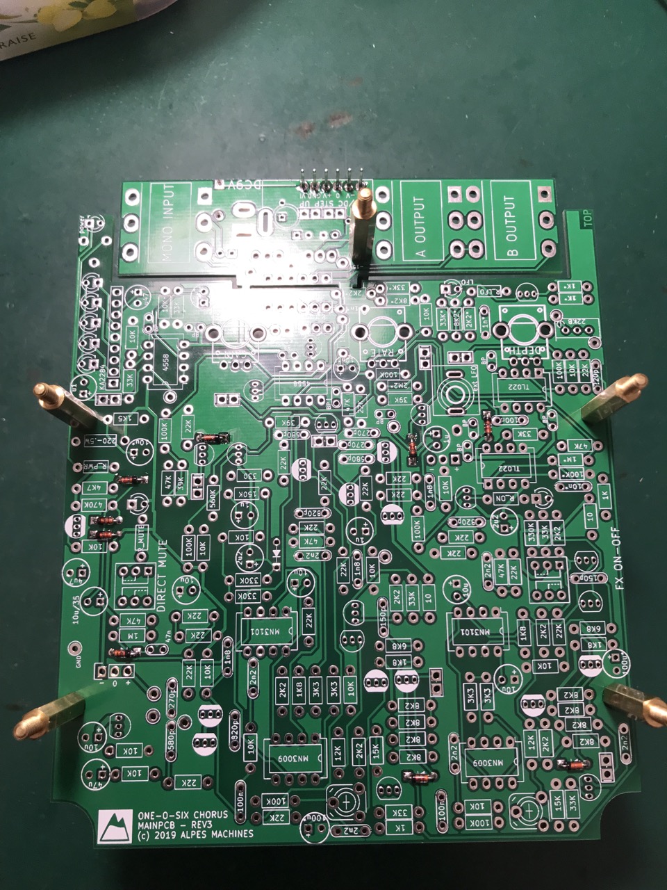
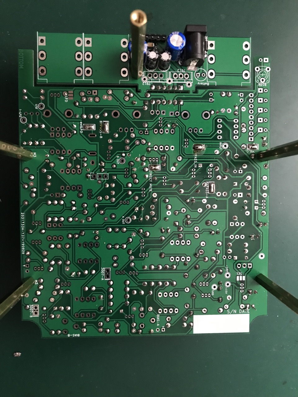
ASSEMBLY OF PCB REV3 and REV3.1 : green PCB
Prepare your board by degreasing it with Isopropyl rubbing Alcohol (IPA).
Solder the 3 SMD 22uF ceramic capacitors if you have got them. Simply put some solder on one pad, place the component with a tweezer, reflow the soldering pad and then solder the other pad. They are not absolutely necessary but the vendor of the DC-DC converter specifies them in the data sheet.

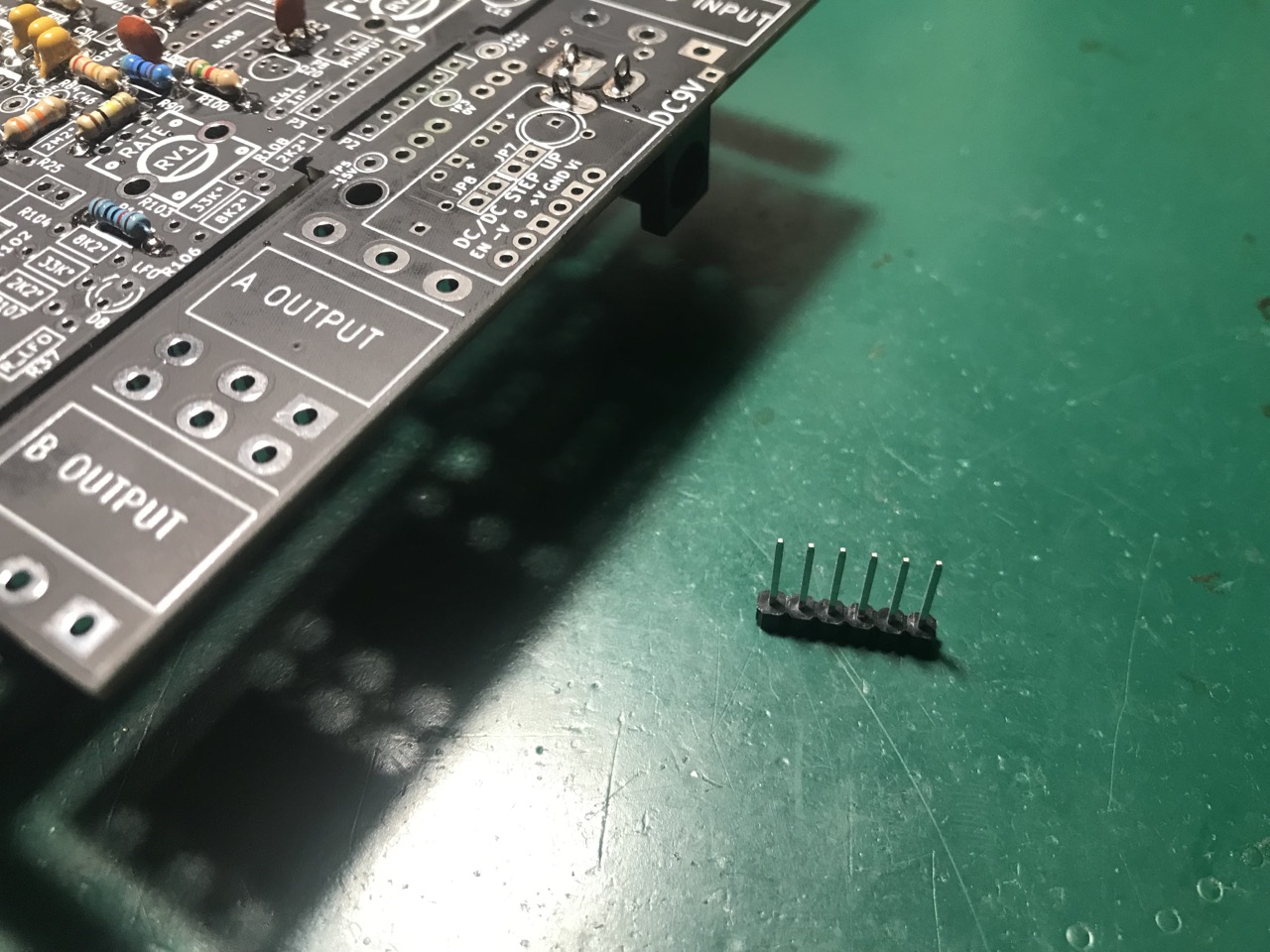
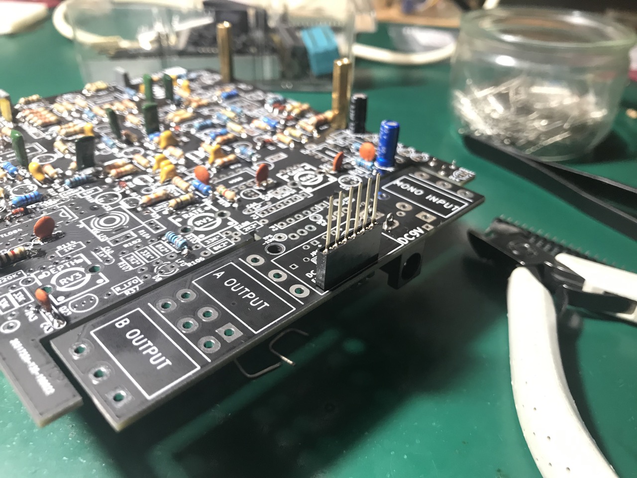
Break the SIL pin header to create a 6-pin-header and fix it to the board as pictured below. This will serve to attach the DC-DC 3W converter to the main board :

Then attach long stand-offs for soldering the resistors and capacitors from the TOP side (faster, no flip of the PCB) :
You are ready to solder diodes and resistors to the mainboard. Insert each component on the top side and let leads go down. You will solder them from the TOP side, a faster method than flipping the PCB for each component :

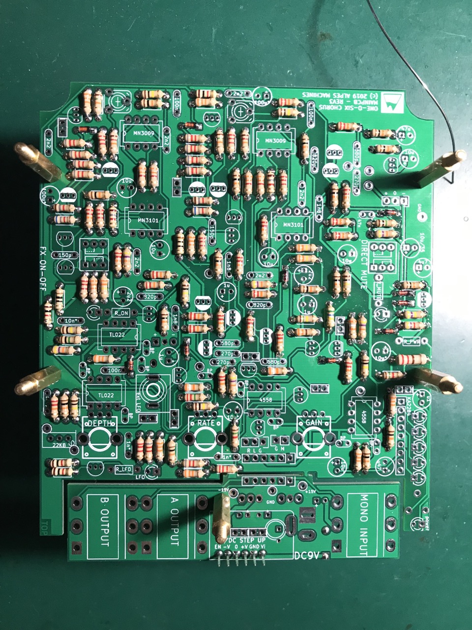

Cut the resistors/diodes leads all at once and then do a 2nd pass to insert ceramic MLCC capacitors. Solder them from the TOP :

Insert electrolytic capacitors but this time you will flip the board to solder these components. Notice you need to push the body of the electro to the maximum on the PCB :


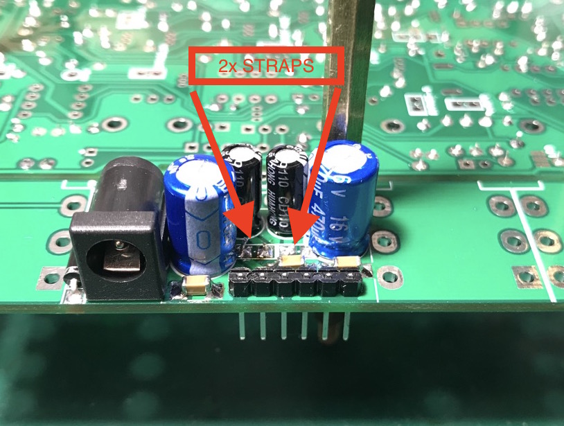
Put a jumper on JP7 & JP8 if you do not use optional voltage regulators 7812 and 7912 :
NOTA : Voltage regulators 78xx and 79xx are used to have a better symmetrical power supply as the DC_DC converter has a -5% difference on negative voltage. We tested both possibilities (within and without the additional regulators) and there is no noticeable difference. The easiest is to use the jumper and not the regulators.
If for some reasons, you prefer to use the voltage regulators 7812 & 7912 all the explanations below relative to a +/-15VDC system won’t be accurate as you power the system with +/-12VDC
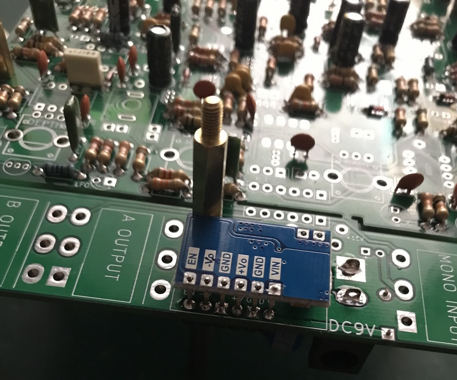
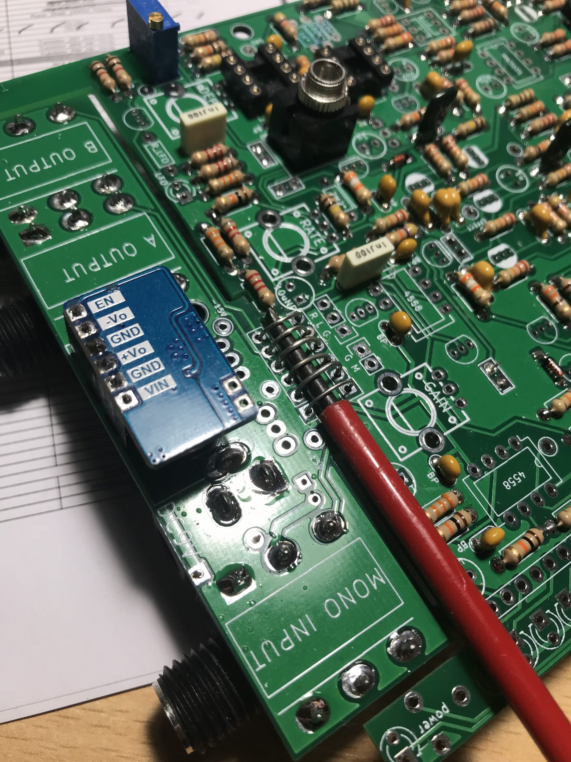
Then solder the DC-DC 3W converter on the pin-header (keep alignement the best you can) :
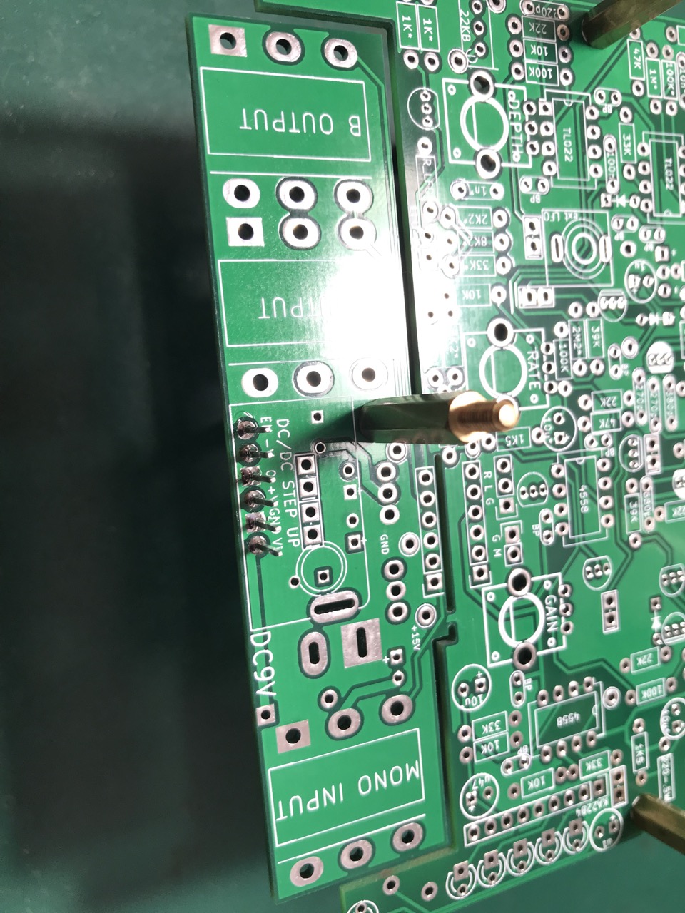
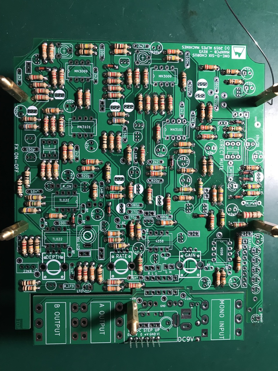
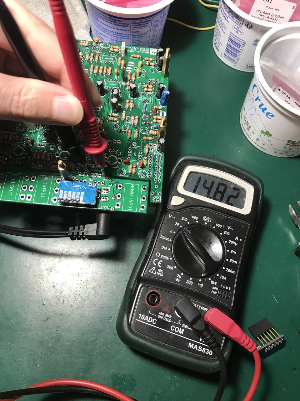
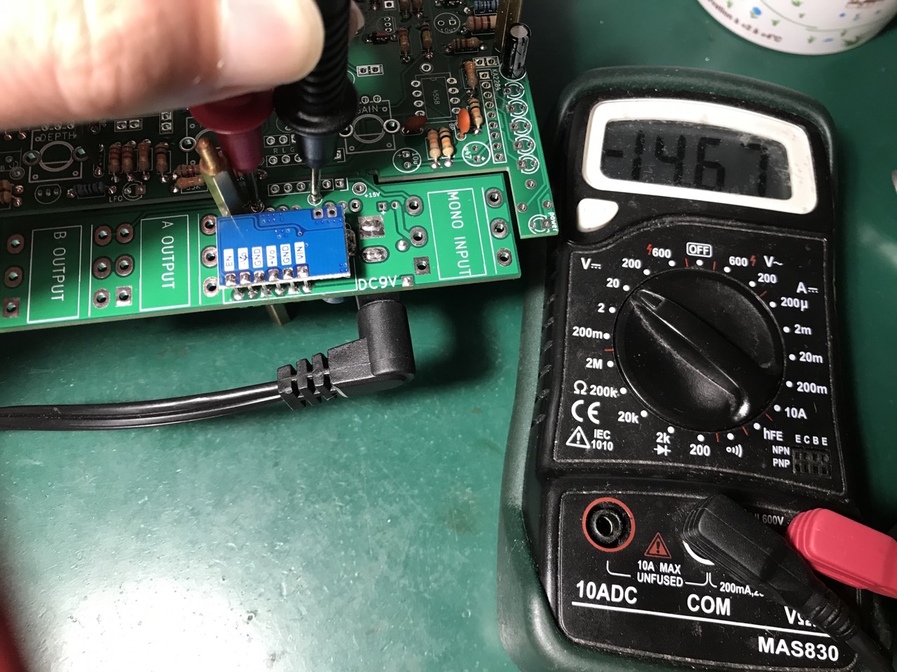
Verify on-board voltages :
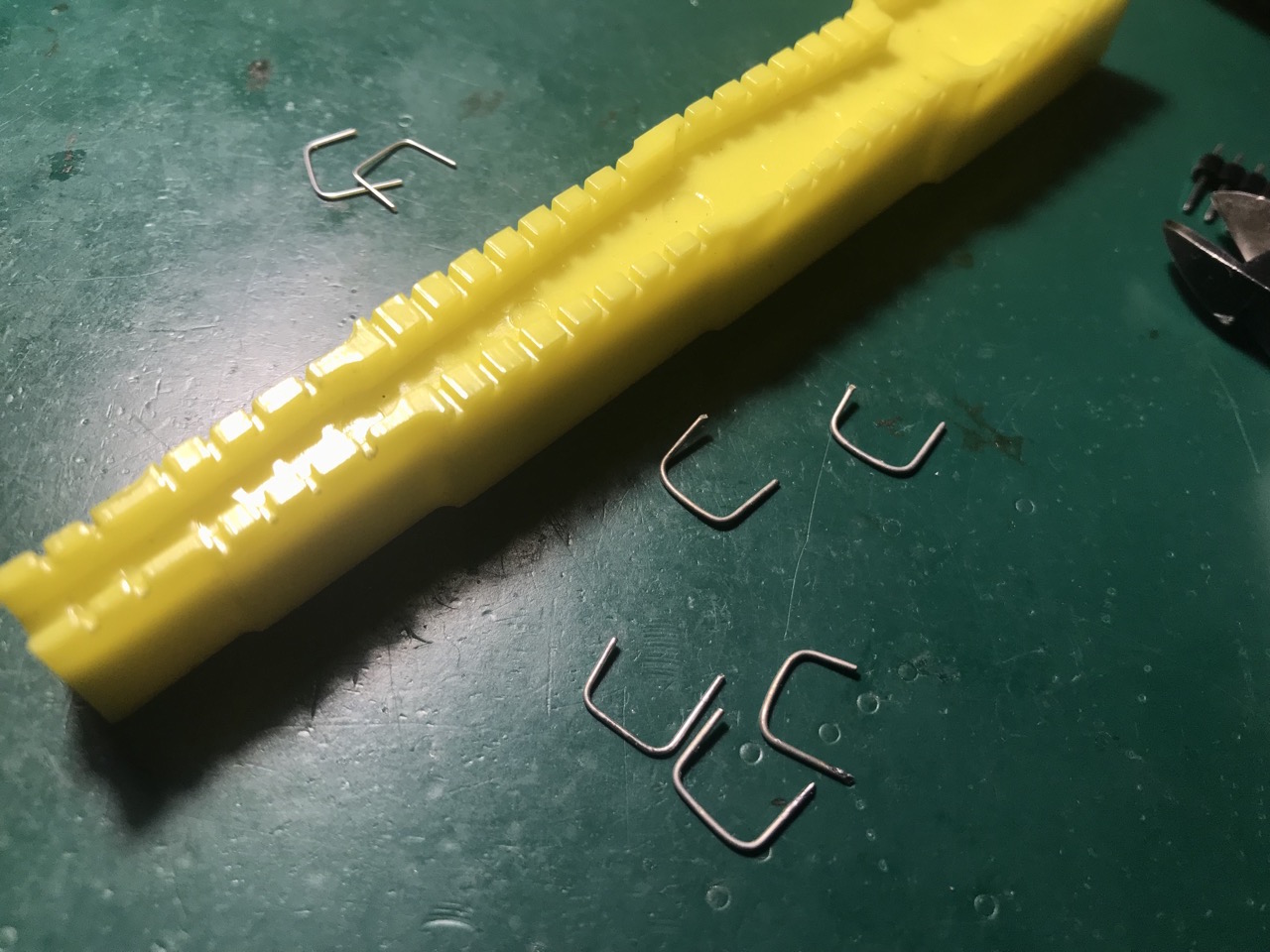
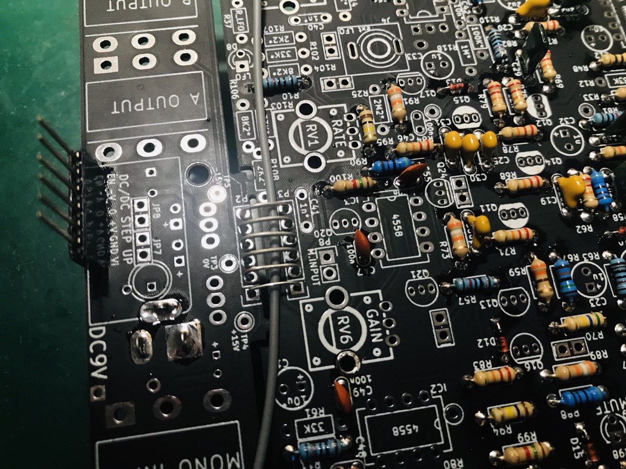
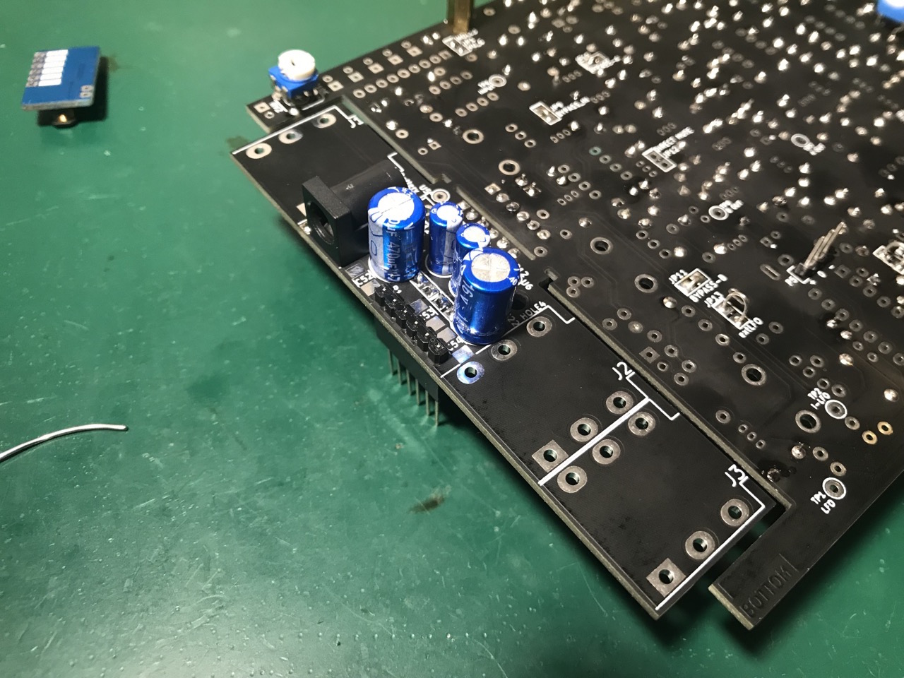
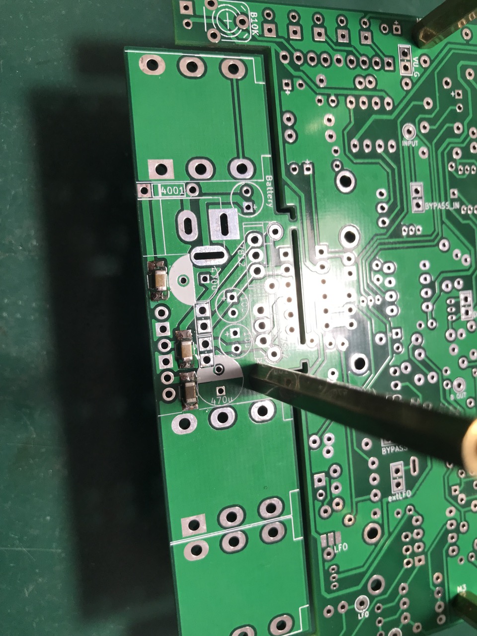
Then create LINKERS using cut resistors leads to link P2 and P3 (MONO IN, +15, GND, -15, LEFT OUT, RIGHT OUT) between the small board and the big one :

Verify voltages on the big board using test points :

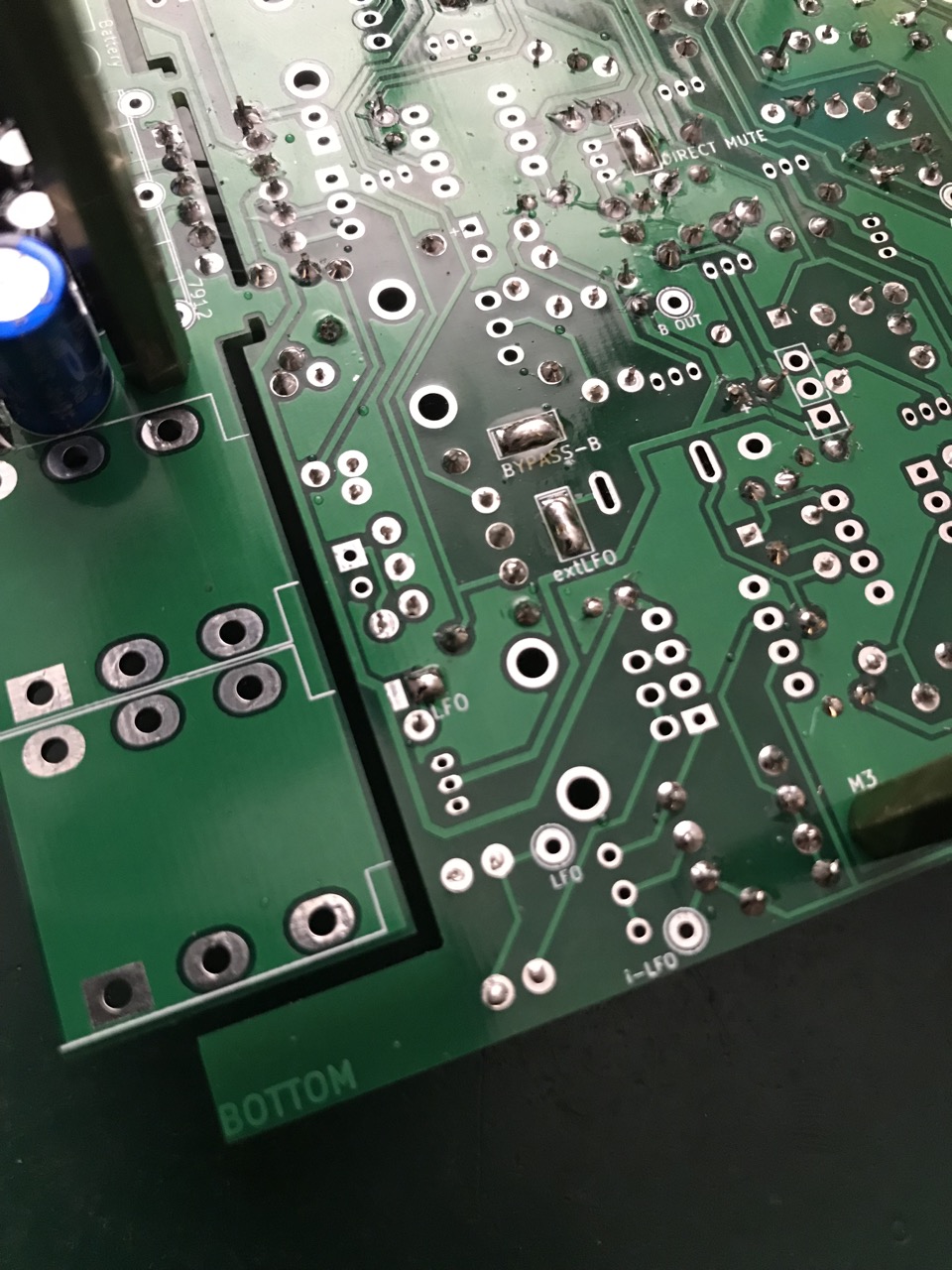
Put solder blobs where necessary :
- SMD jumper LFO : select the “ground” of the Modulator’s LED,
- SMD jumper SEL : voltage pump for the output stage (copied from Juno 106)


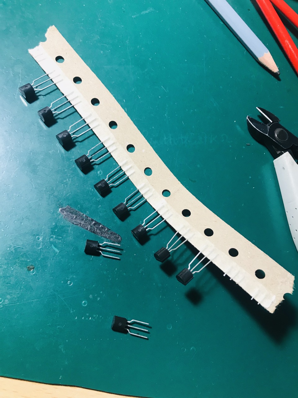
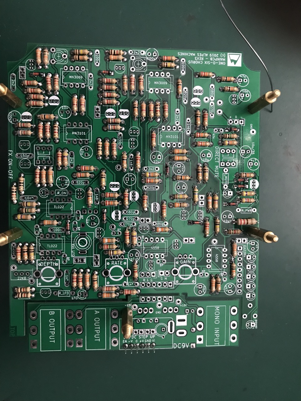
Place the DIP-8 sockets for the integrated circuits. Solder the transistors.
Place the MN3007 jumpers if you are using MN3007 BBD – leave free if MN3009. You can use previously cut resistors leads (jumpers have holes to insert the lead).
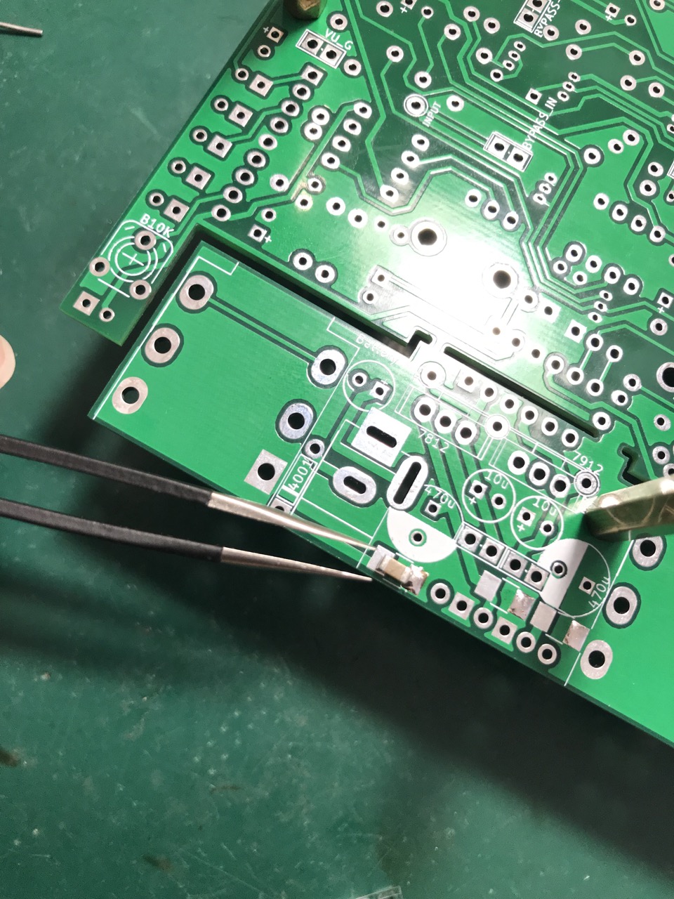
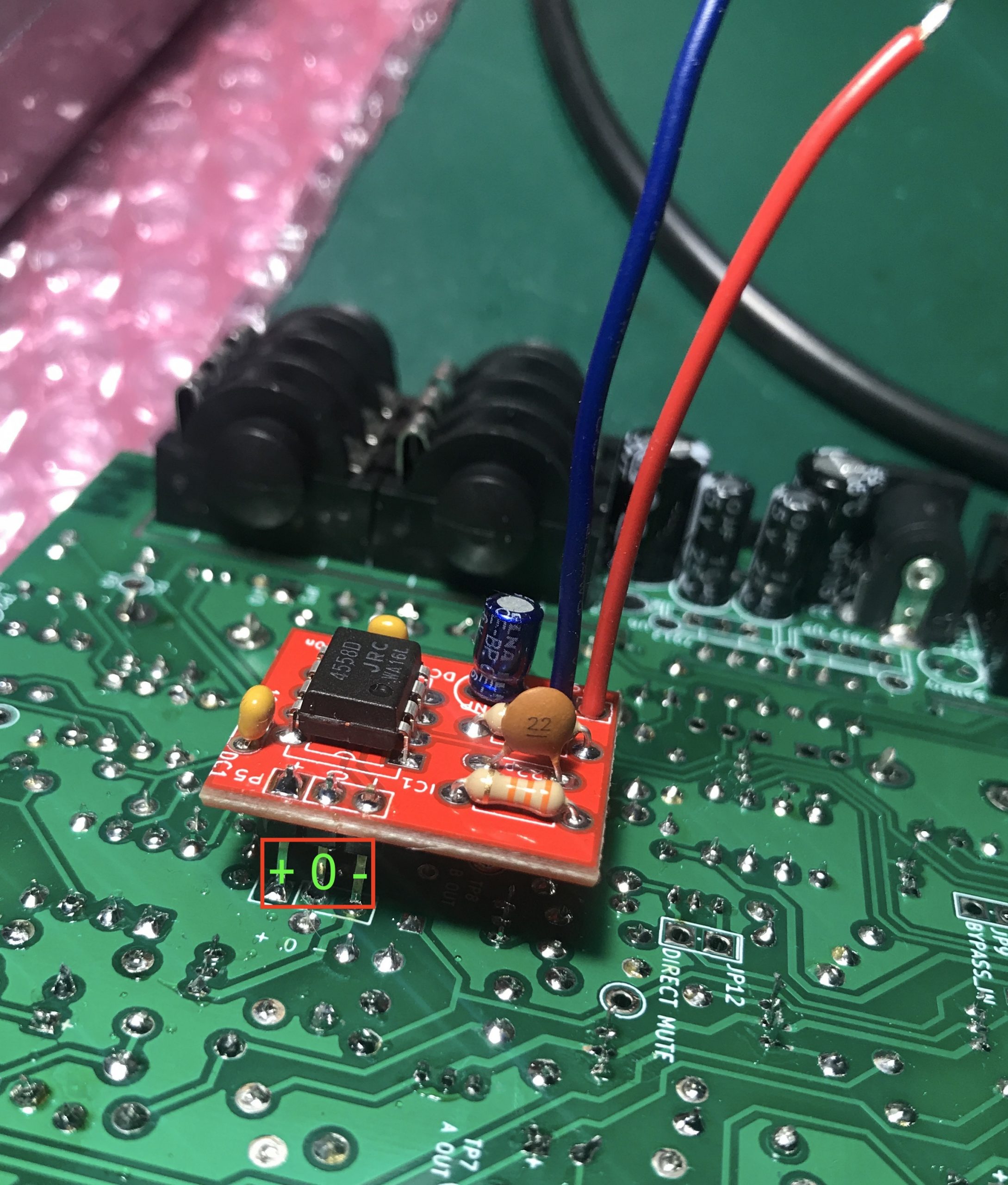
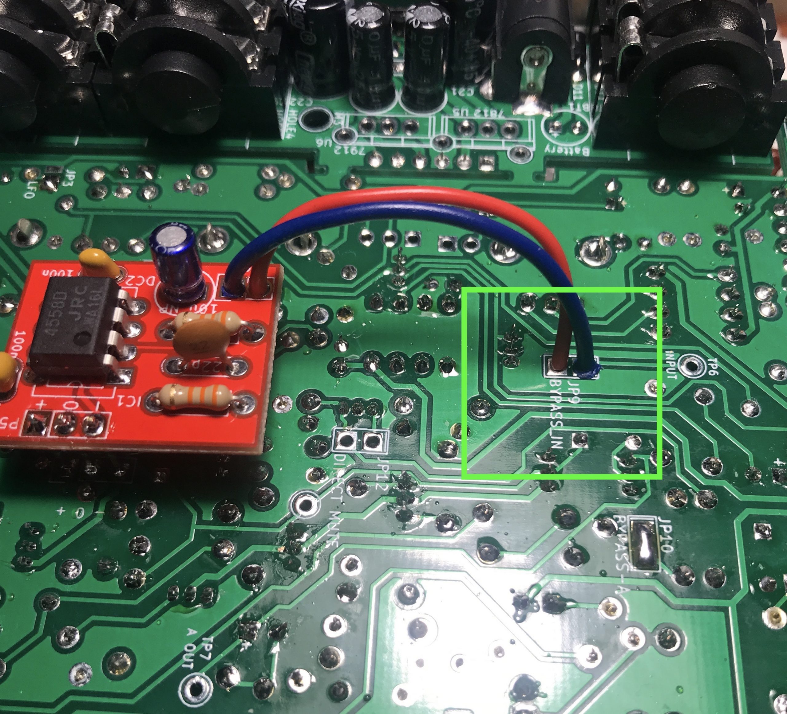
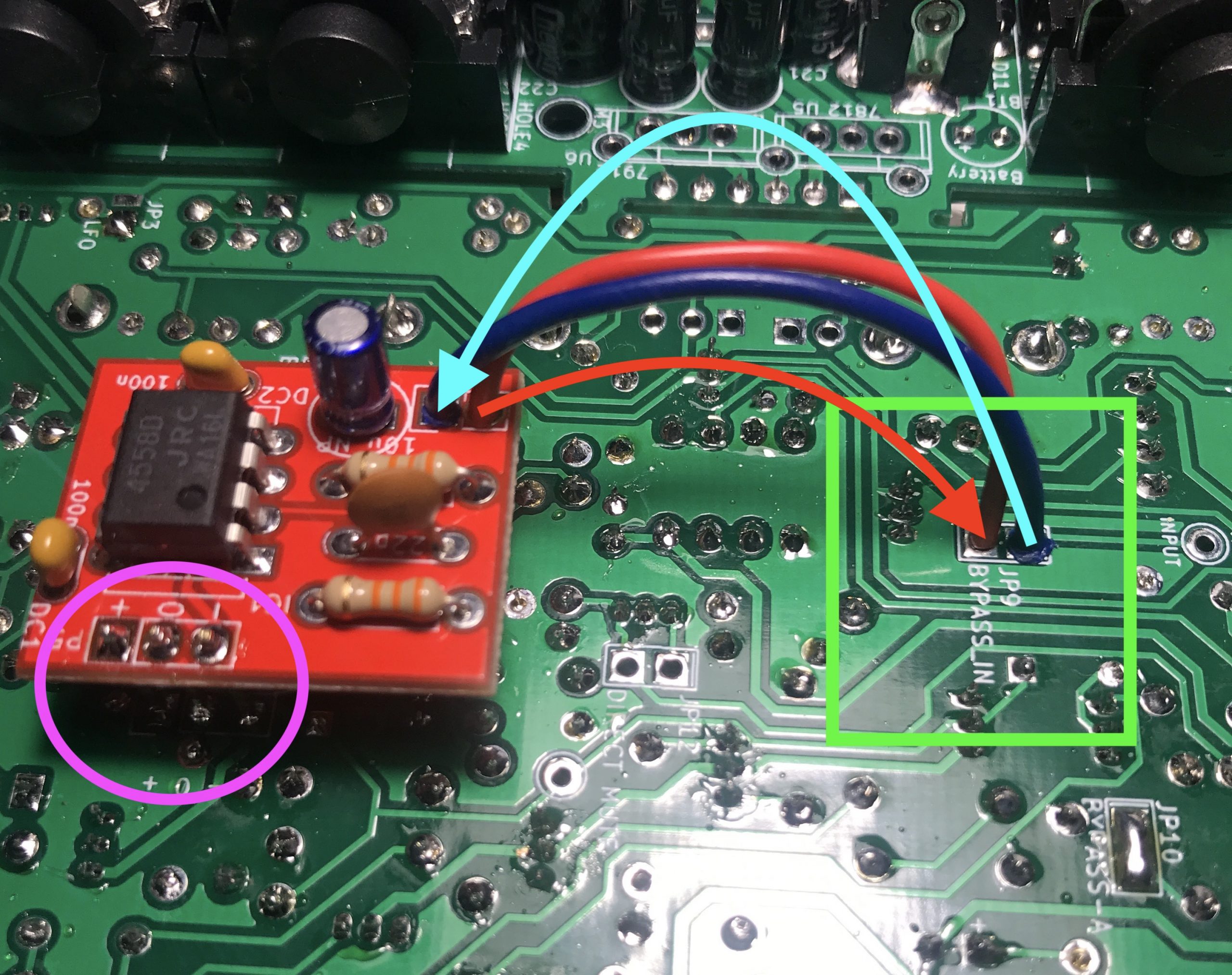
SMALL PCB AOP INV
Since July 2022, you will find an additional small PCB (AOP_INV). It is an additional AOP inverter in the signal chain to get a perfect in phase signal between INPUT and OUTPUTS.
Parts needed :
- 1x 10uF Non Polarised electrolytic capacitor
- 2x 33K resistors
- 1x 22pF capacitor (any material)
- 1x 4558 or TL072 OpAmp
- 2x 100nF bypass capacitors (any material)
- 2x wires
- 1x 3pins header 0,254″
If you omit it you won’t ear any difference. It is just to be mathematically perfect in terms of phase in the audio path (180° rotation -> AOP INV -> 0° rotation).
You will insert it inside JP9, replacing the jumper or the solder blob, directly powered by the +0- next to J9 :
Final result : 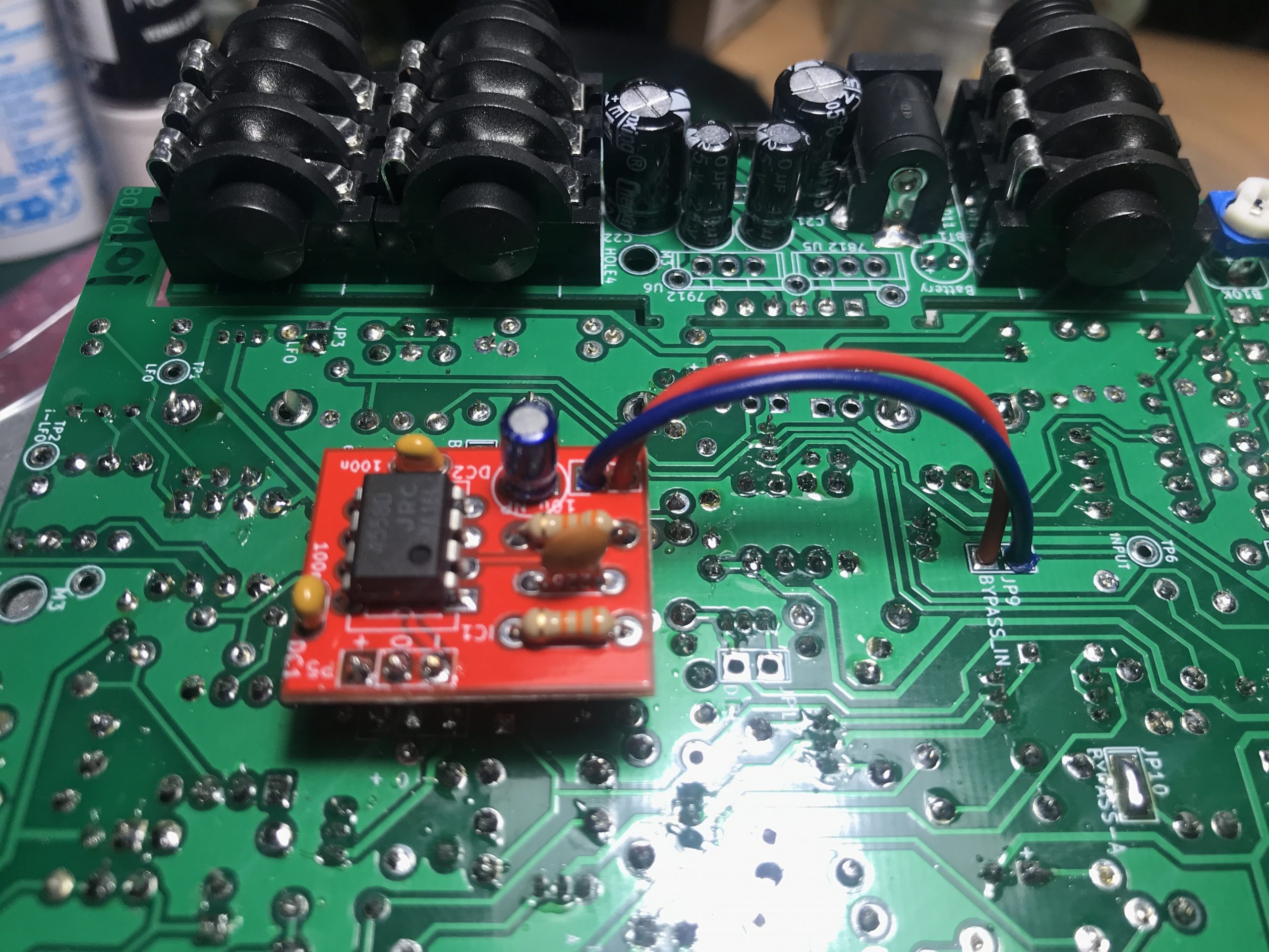
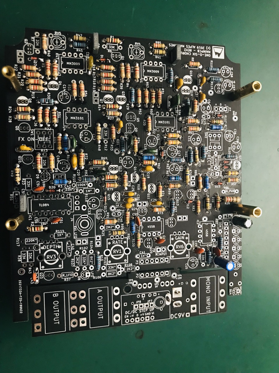
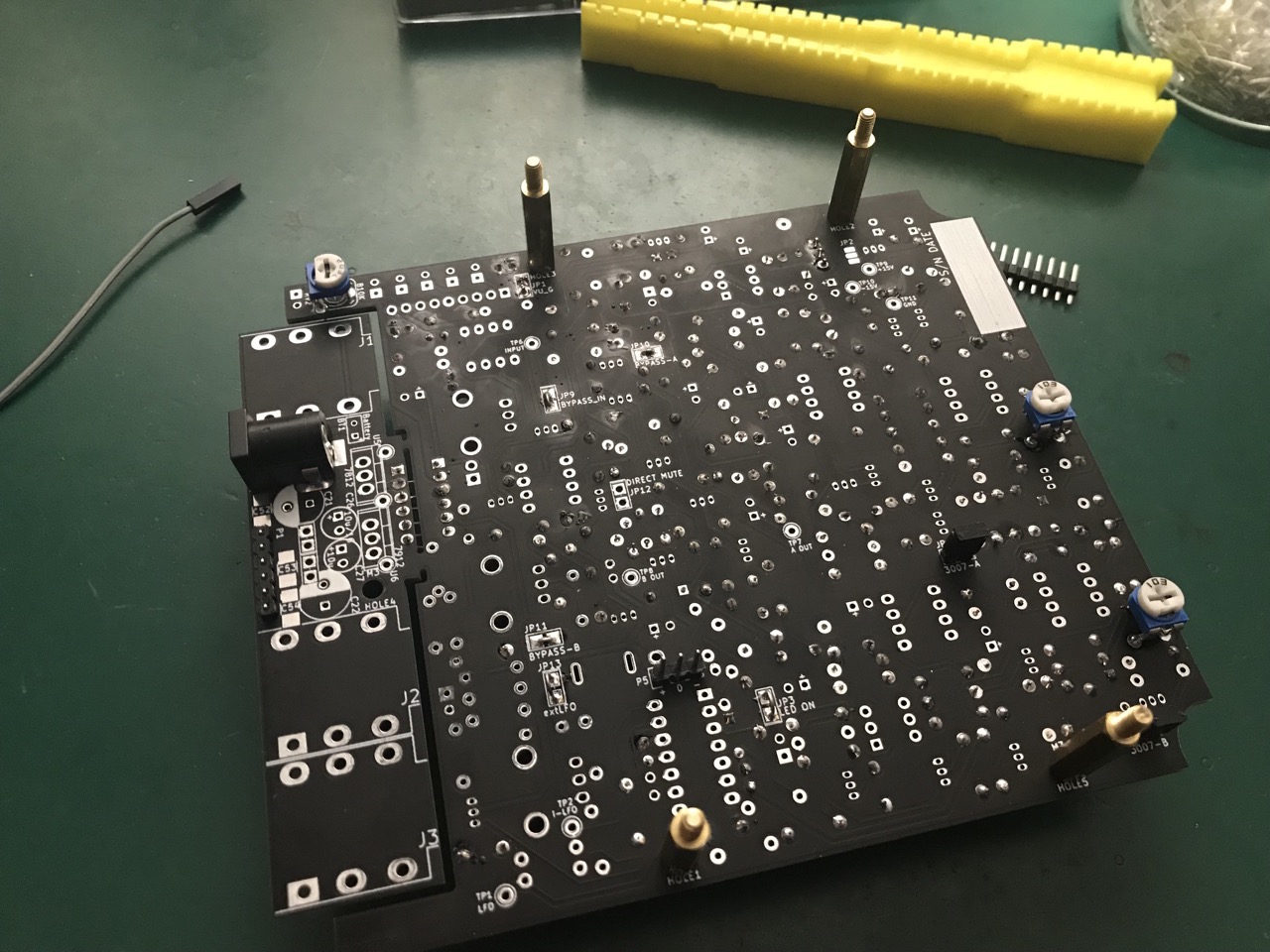
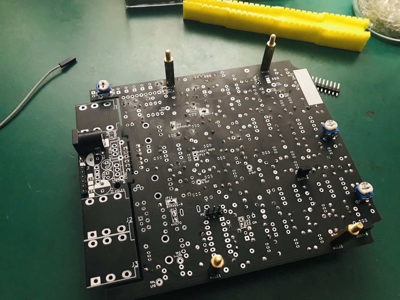
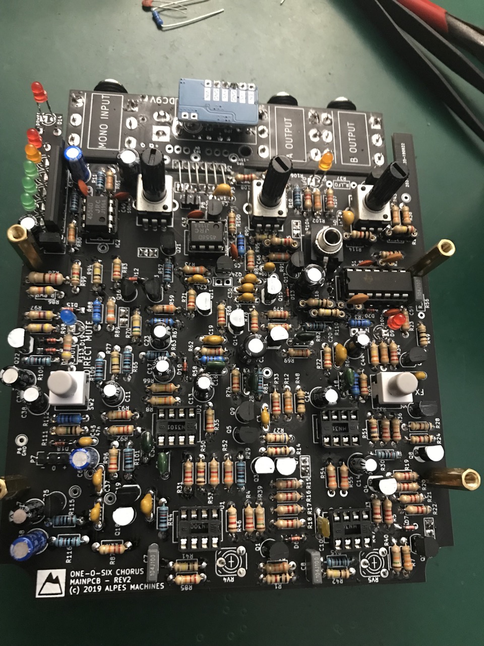
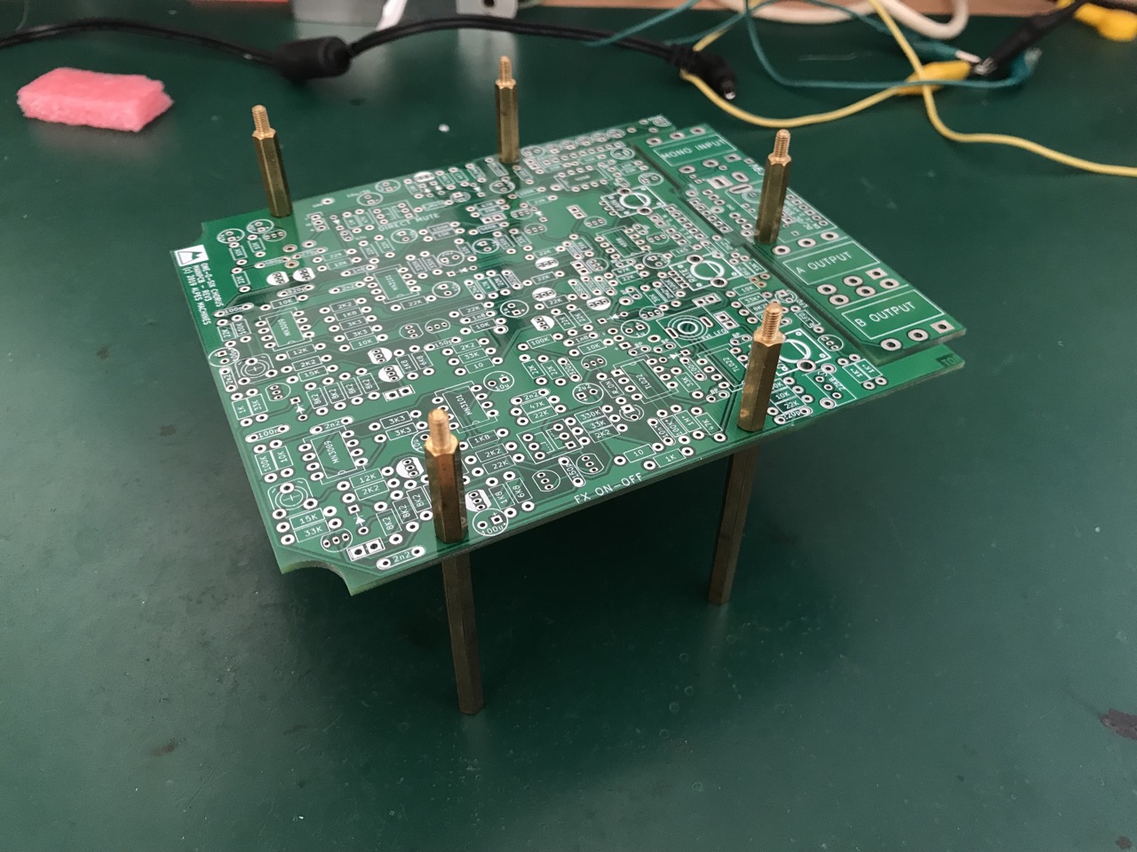
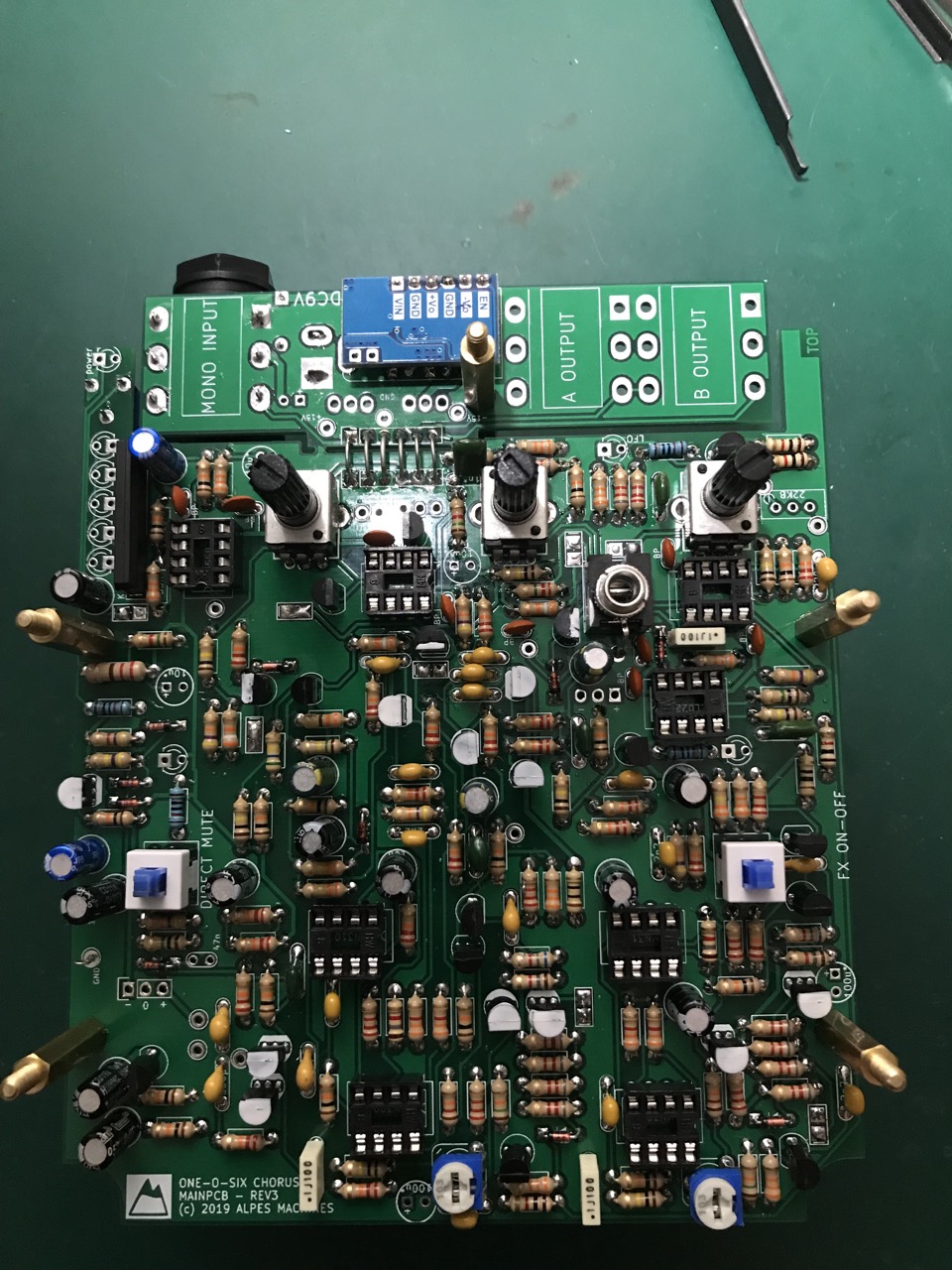
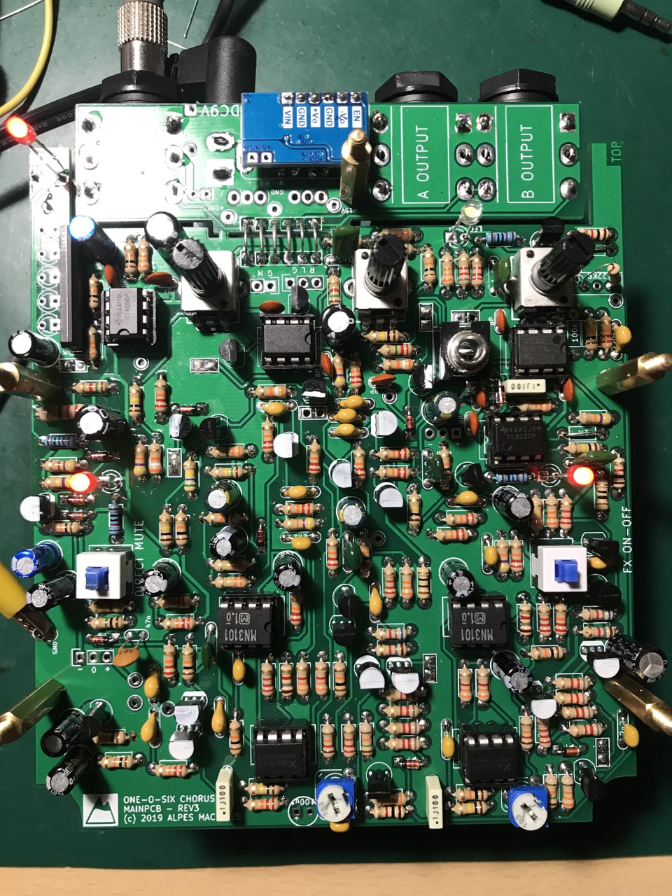
Finished assembled board REV3 :
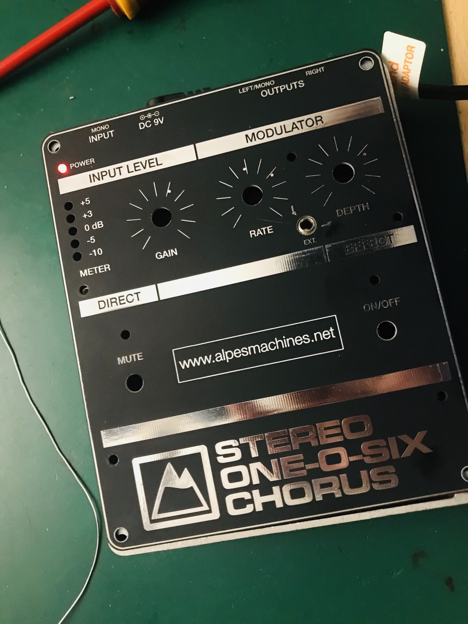
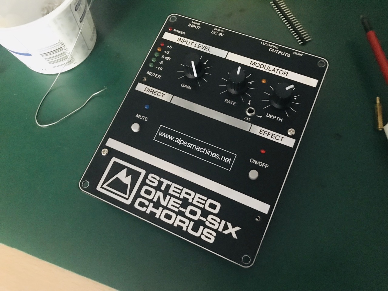
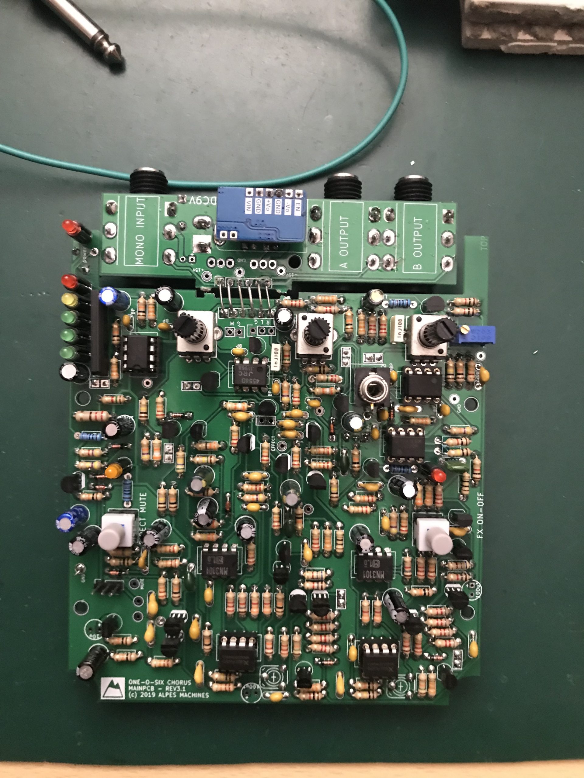
Finished Product assembly :
CALIBRATION
It is now time to calibrate your unit : the Meter section, the inverted LFO amplitude and the Bias, Bias-A corresponding to the chorus Left channel, and Bias-B to the Right.
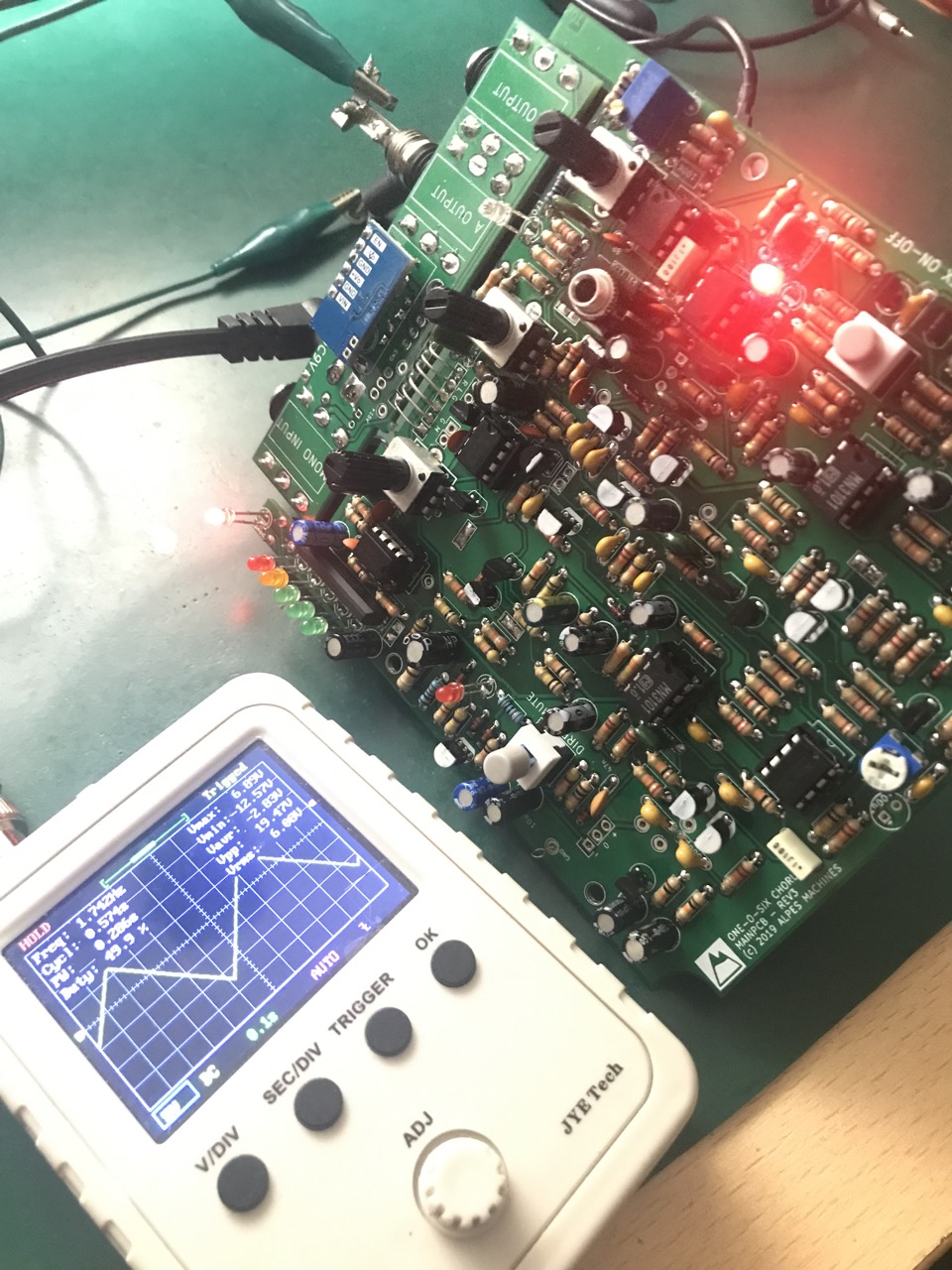
Calibrating LFO on-board Modulator :
Turn Depth and Rate fully clockwise to get the fatest modulator possible (this helps to read low frequencies on Digital Oscilloscope). We use a DSO150 pocket oscilloscope (20-30€ on the internet) in the pictures.
Trim RV7 to adjust the amplitude of i-LFO : same amplitude as LFO with a 180° phase rotation, 20Vpp (19,67V in the picture) as specified in Roland Juno 106 Service Manual.

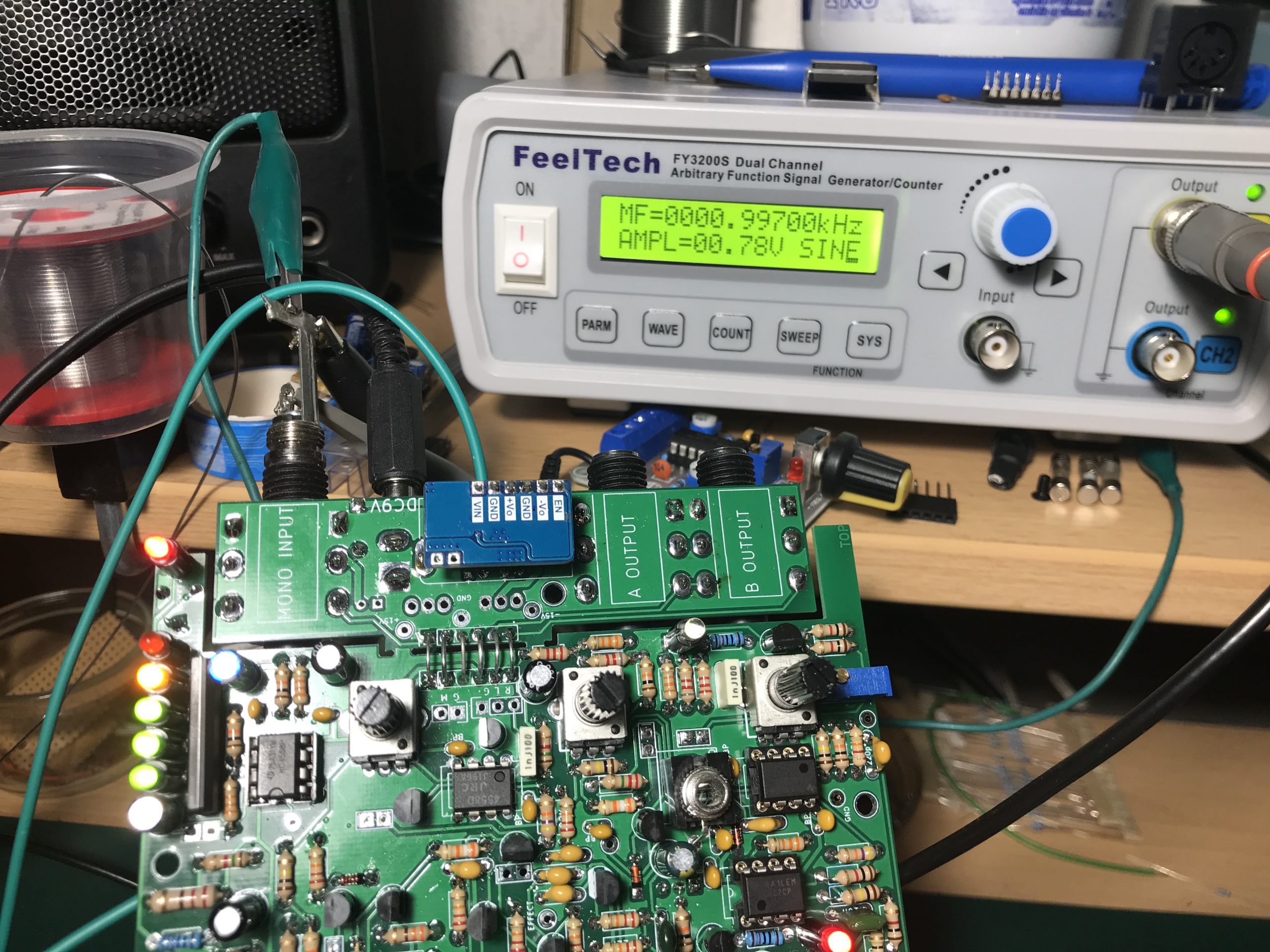
Calibrating VU meter :
Ideally you will have a small oscilloscope and a waveform generator (your DAW is perfect for that) connected to MONO IN or P8. This can also be made by ears. Program a low level sinus 440Hz in your DAW. Insert this signal to the Mono Input of the Chorus.
Turn fully clockwise the INPUT Gain knobs.
Process : use a sinus or triangle input test signal and monitor it until it saturates the BBD stage (TP7, TP8). This will give you the max level input the One-O-Six can support, corresponding to the LEVEL Red LED.
Listen to the result with EFFECT On and DIRECT not muted.
Turn INPUT Gain at 2 o’clock.
Adjust the vu meter trimmer to have VU meter red LED lit. This way you still have some dB before overdriving the BBD.
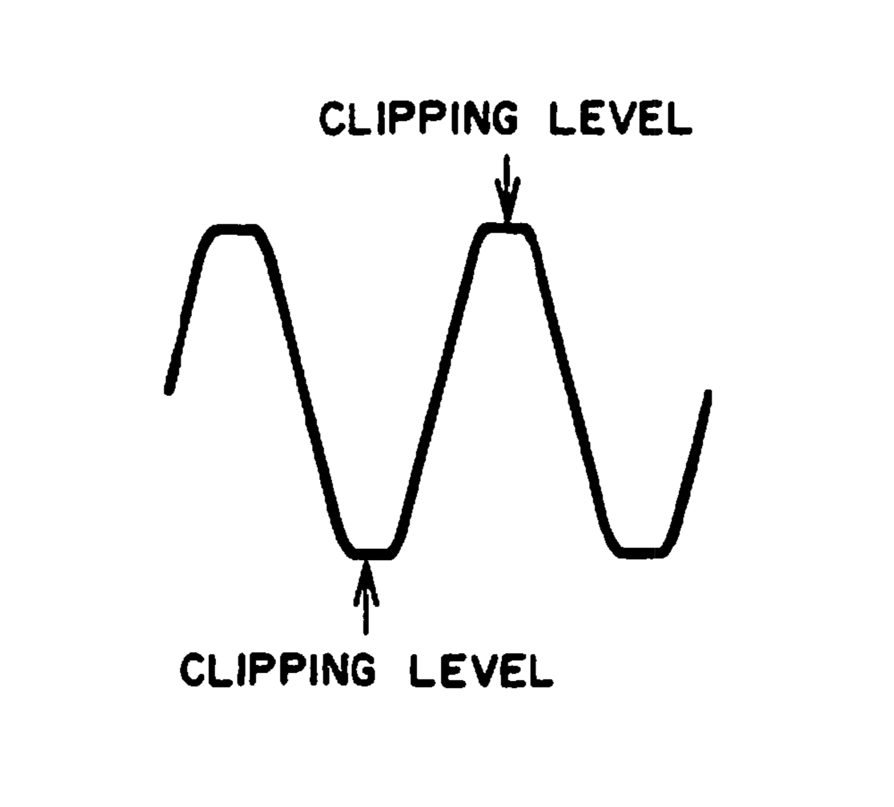
CHORUS BIAS = Calibrating the left and right BBD sections which are the chorus signal :
BBD MN300x chipsets have a variable voltage input range. Each chipset has its own characteristic, so you need to adapt the circuitry to the chipset. This is done by introducing a bias voltage to the signal on the input (pin3 of MN300x, see schematic).
We will inject that bias voltage (some negative DC voltage) into the test signal by turning the trimmers to perfectly align the center of the test signal around 0V as depicted in Roland Juno 106 service manual. The negative peak and the positive peak of the sinusoidal signal must be symmetrical :

- Turn fully clockwise depth and Rate
- Follow process described in the Juno 106 service Manual
- Roland Juno-106 Service Manual
- Turn Bias-A trimmers to adjust channel A (Left) while monitoring TP7
- Turn Bias-B trimmers to adjust channel B (Right) while monitoring TP8
**Monitoring the signal – BEFORE**
The test chorused signal is asymmetrical around zero (top peak normal, bottom peak overdriven) :

**Monitoring the signal – AFTER**
You introduce some voltage bias by turning the trimmer to make it symmetrical around zero with peaks less saturated. You can hear the signal is more “pure” :

Bias-A and Bias-B trimmers are usually at 11 o’clock :

Check that the LEVEL display is still OK (saturation when red, no saturation when green) and repeat the process if necessary.
ENCLOSURE
You can eventually break the PCB to give a small angle to the Jacks in order to to fit & stick to the enclosure, but it appears that it is working as is.
**picture break PCB**
Insert the populated PCB inside the 1590XX enclosure and tighten jacks plastic nuts.
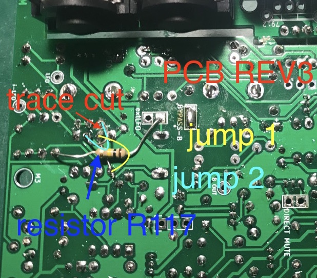
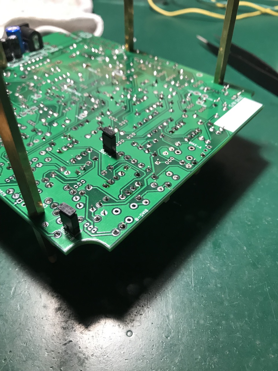
PCB REV3 modification (not sold in the shop, FYI) :
We made an error while routing the modulator as we used the same NET name in Kicad. Simply cut one trace and make two jumper wires. Populate R117 on the PCB bottom side. Error solved in rev3.1